WORKSHOP PAPER
CMOS Image Sensors and Plasma Processes : How PMD Nitride Charging Acts on The Dark Current
Abstract
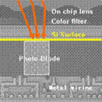
This study focuses on how the dark current in a Front-Side Illuminated (FSI) sensor is affected by interface damages and charges in the Pre-Metal Dielectrics (PMD) stack, due to plasma processes. The experimental setup includes characterizing potential and charge in dielectrics using the Corona Oxide Characterization Of Semiconductor (COCOS) technique and TCAD simulations to illustrate the link between dark current and dielectrics characterization results. The findings indicate that plasma processes induce significant variations in dark current by trapping positive and negative charges in the PMD nitride layer, thereby affecting the oxide/silicon interface passivation.Keywords
CMOS Image Sensors, PMD Nitride Charging, Dark Current,References
1) K. Tokashiki et al., "Study of plasma charging-induced white pixel defect increase in CMOS active pixel sensor", Thin Solid Films, 2007. https://doi.org/10.1016/j.tsf.2006.10.065
2) J. P. Carrère et al., "New mechanism of plasma induced damage on CMOS image sensor: Analysis and process optimization", Solid. State. Electron., 2011. https://doi.org/10.1016/j.sse.2011.06.037
3) M. Wilson, "COCOS (corona oxide characterization of semiconductor) non-contact metrology for gate dielectrics", AIP Conf. Proc., 2001. https://doi.org/10.1063/1.1354401
4) H. Haug, S. Olibet, Ø. Nordseth, and E. S. Marstein, "Modulating the field-effect passivation at the SiO2/c-Si interface: Analysis and verification of the photoluminescence imaging under applied bias method", J. Appl. Phys., 2013. https://doi.org/10.1063/1.4827417
5) V. Sharma et al, "Study and manipulation of charges present in silicon nitride films", IEEE 39th Photovoltaic Specialists Conference (PVSC), 2013. https://doi.org/10.1109/pvsc.2013.6744377
6) H. Sinha, J. L. Lauer, G. A. Antonelli, Y. Nishi, and J. L. Shohet, "Charging response of back-end-of-the-line barrier dielectrics to VUV radiation", Thin Solid Films, 2012. https://doi.org/10.1016/j.tsf.2012.04.014
7) R. J. Powell and G. F. Derbenwick, "Vacuum ultraviolet radiation effects in SiO2 (Vacuum UV irradiation of silicon dioxide, discussing positive charging for photon energies above threshold for electron-hole pair creation)", IEEE Trans. Nucl. Sci., 1971
8) C. Cismaru and J. L. Shohet, "In situ electrical characterization of dielectric thin films directly exposed to plasma vacuum-ultraviolet radiation", J. Appl. Phys., 2000. https://doi.org/10.1063/1.1305836
9) Y. Takahashi, K. Ohnishil, T. Fujimakil, and M. Yoshikawaz, "Radiation-induced trapped charge in metal-nitride-oxide-semiconductor structure", IEEE Trans. Nucl. Sci., 1999. https://doi.org/10.1109/23.819124
10) W. Shockley and W. T. Read, "Statistics of the Recombination of Holes and Electrons", Phys. Rev., 1952. https://doi.org/10.1103/physrev.87.835


