WORKSHOP PAPER
World first mass productive 0.8㎛ pixel size image sensor with new optical isolation technology to minimize optical loss for high sensitivity
Abstract
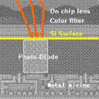
More and more pixels are needed to implement CMOS image sensors with high resolution while reducing the size of the chips. As the beam size of the incoming light nears the pixel size, the light loss from the conventional metallic grid increases. Development of an architecture that minimizes optical losses is key technology to secure pixel performance of sub-micro sized pixel. In this paper, we analyzed the light loss according to the pixel size and the optical structure. Based on this, we are going to introduce a new isolation structure that minimizes optical losses applied to the world's first 0.8um pixel size product.Keywords
CMOS image sensors, optical losses, ISOCELL PLUS,References
1) Y. Kim et al., "A 1/2.8-inch 24M pixel CMOS image sensor with 0.9㎛ pixels separated by full-depth trench isolation", Proc. ISSCC, Jan., 2018, 2018. https://doi.org/10.1109/isscc.2018.8310195
2) S. Choi et al., "An all pixel PDAF CMOS image sensor with 0.64㎛ x 1.28㎛ photodiode separated by self-aligned in-pixel deep trench isolation for high AF performance", IEEE Symp., VLSI Tech., Jun., 2017, 2017. https://doi.org/10.23919/vlsit.2017.7998212


